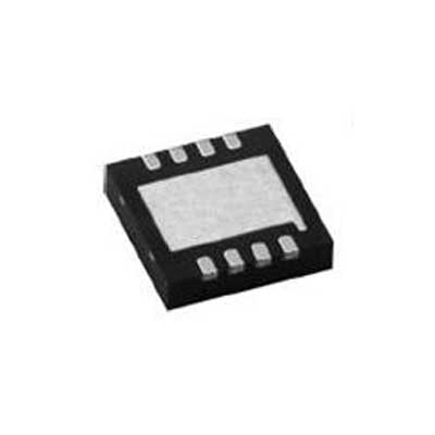
Power Switch/Driver 1:1 N-Channel 4A 8-WSON (2x2)
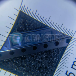


图片仅供参考.
有关产品详细信息,请参阅产品规格。
Power Switch/Driver 1:1 N-Channel 4A 8-WSON (2x2)
订单满$200即可获赠限量版中式礼品一份.
订单金额超过 1000 美元可减免 30 美元运费.
超过 5000 美元的订单可免运费和交易费.
这些优惠适用于新客户和现有客户,有效期为2024年1月1日至2024年12月31日.
TI
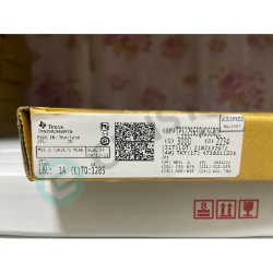
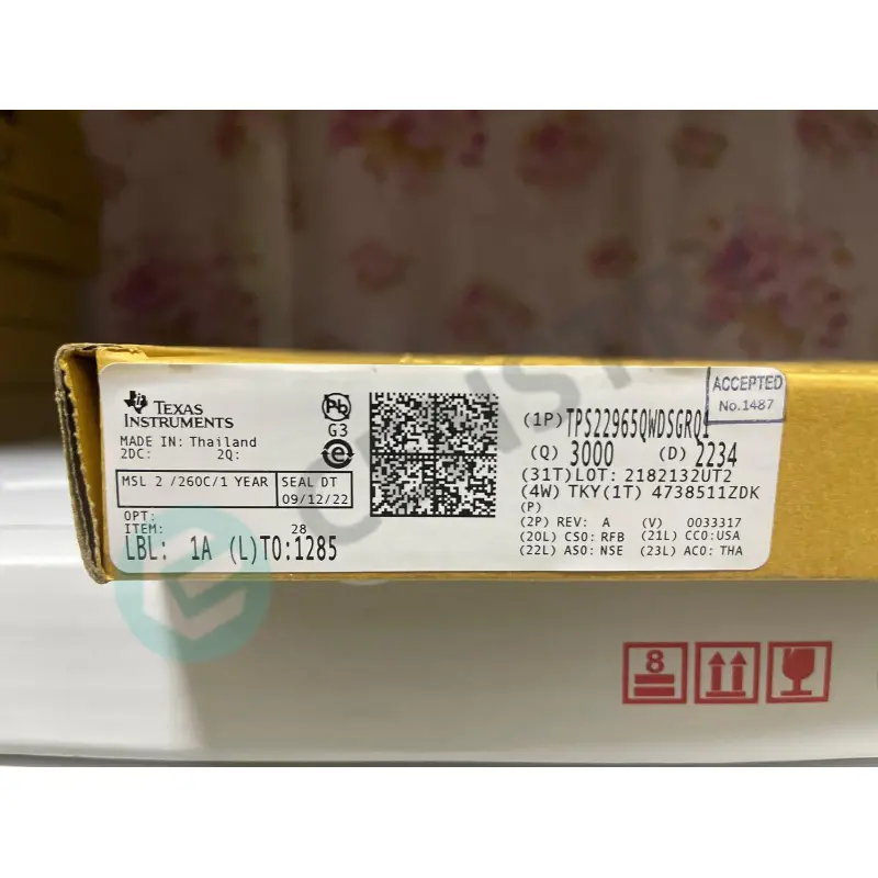
TPS22965QWDSGRQ1 datasheet
WSON-8
射频集成电路
 Lead free/RoHS Compliant
现在提交您的报价请求,我们期望在 五月 04, 2024内提供报价。现在就下订单,我们期望在 五月 09, 2024内完成交易。时间是格林威治标准时间+8:00。


1 Features
• Qualified for automotive applications
– AEC-Q100 qualified
– Device temperature grade 2: –40°C to +105°C
(TPS22965-Q1, TPS22965N-Q1)
– Device temperature grade 1: –40°C to +125°C
(TPS22965W-Q1, TPS22965NW-Q1)
– Device HBM ESD classification level 3A
– Device CDM ESD classification level C6
• Functional Safety-Capable
– Documentation available to aid functional safety system design
• Integrated single channel load switch
• Input voltage range: 0.8 V to 5.5 V
• Ultra-low on resistance (RON)
– RON = 16 mΩ at VIN = 5 V (VBIAS = 5 V)
– RON = 16 mΩ at VIN = 3.6 V (VBIAS = 5 V)
– RON = 16 mΩ at VIN = 1.8 V (VBIAS = 5 V)
• 4-A maximum continuous switch current
• Low quiescent current (50 µA)
• Low control input threshold enables use of 1.2-, 1.8-, 2.5- and 3.3-V logic
• Configurable rise time
• Quick Output Discharge (QOD) (TPS22965-Q1 and TPS22965W-Q1 only)
• WSON 8-pin package with thermal pad
2 Applications
• Automotive electronics
• Infotainment
• ADAS (Advanced Driver Assistance Systems)
3 Description
The TPS22965x-Q1 is a small, ultra-low-RON, singlechannel load switch with controlled turn-on. The device contains an N-channel MOSFET that can operate over an input voltage range of 0.8 V to 5.5 V and can support a maximum continuous current of 4 A. The VOUT rise time is configurable so that
inrush current can be reduced. The TPS22965-Q1 and TPS22965W-Q1 devices include a 225-Ω on-chip
load resistor for quick output discharge when the switch is turned off.
The TPS22965x-Q1 devices are available in a small, space-saving 2-mm × 2-mm 8-pin WSON package (DSG0008A) with integrated thermal pad allowing for high power dissipation. The TPS22965-Q1 and TPS22965N-Q1 devices are characterized for operation over the free-air temperature range of –40°C to 105°C. Furthermore, the TPS22965WQ1 and TPS22965NW-Q1 devices feature wettable flanks in the same WSON package (DSG0008B) and it is characterized for operation over the free-air temperature range of –40°C to +125°C.

Request a quote TPS22965QWDSGRQ1 at censtry.com. All items are new and original with 365 days warranty! The excellent quality
and guaranteed services of TPS22965QWDSGRQ1 in stock for sale, check stock quantity and pricing,
view product specifications, and order contact us:sales@censtry.com.
The price and lead time for TPS22965QWDSGRQ1 depending on the quantity required, please send your request to us,
our sales team will provide you price and delivery within 24 hours, we sincerely look forward to cooperating with you.

Fremont
6921 PCS
FT24C64A-UNR-T .PDF
Fremont
5373 PCS
FT24C08A-ULR-T .PDF
Fremont
3772 PCS
FT24C32A-USR-T .PDF
Fremont
3000 PCS
FT93C66A-USR-T .PDF
2024-05-03
It is a pleasure doing business with Censtry.
2024-05-03
Good and trustable Company
2024-05-03
I trust this company, very good reputation.
2024-05-03
Good company, great customer services and honest. I look forward to working with you guys again :)
2024-05-02
Good credit!Nice partner!
2024-05-02
Great company. Quality product.
2024-04-30
GOOD SUPPLIER - A+
2024-04-28
Great and reliable company, pleasure to deal with Avi...thanks
2024-04-22
Great company to deal with, always a pleasure to do business with Bryan. Hope we can do more business in the future.
2024-04-12
Great Company, nice to work with.Thank you very much Imraan
我们高度重视您的反馈意见。请分享您最真实的评价。
*请在发表评论之前登录您的帐户