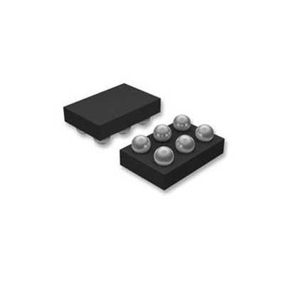
Power Switch/Driver 1:1 N-Channel 3A 6-DSBGA


图片仅供参考.
有关产品详细信息,请参阅产品规格。
Power Switch/Driver 1:1 N-Channel 3A 6-DSBGA
订单满$200即可获赠限量版中式礼品一份.
订单金额超过 1000 美元可减免 30 美元运费.
超过 5000 美元的订单可免运费和交易费.
这些优惠适用于新客户和现有客户,有效期为2024年1月1日至2024年12月31日.
TI
TPS22925CNYPHR datasheet
DSBGA-6
射频集成电路
 Lead free/RoHS Compliant
现在提交您的报价请求,我们期望在 五月 05, 2024内提供报价。现在就下订单,我们期望在 五月 08, 2024内完成交易。时间是格林威治标准时间+8:00。


1 Features
• Input Voltage Range: 0.65 V to 3.6 V
• On-Resistance
– RON = 9.2 mΩ at VIN = 3.6 V
– RON = 9.2 mΩ at VIN = 1.8 V
– RON = 10.2 mΩ at VIN = 1 V
– RON = 13.1 mΩ at VIN = 0.65 V
• 3-A Maximum Continuous Switch Current
• Quiescent Current, IQ,VIN = 29 µA at VIN = 3.6 V
• Low Control Input Threshold Enables 1.5-, 1.8-, 2.5-, or 3.3-V Logic
• Controlled Slew Rate
– tR = 97 µs at VIN = 3.6 V (TPS22925Bx)
– tR = 810 µs at VIN = 3.6 V (TPS22925Cx)
• Reverse Current Blocking (When Disabled)
• Quick Output Discharge (QOD) (TPS22925B and TPS22925C only)
• Wafer Chip Scale Package:
– 0.9 mm x 1.4 mm, 0.5-mm Pitch, 0.4-mm Height
• ESD Performance Tested per JESD 22
– 2-kV HBM and 1-kV CDM
2 Applications
• Computing
• SSD
• Tablets
• Wearables
• EPOS
3 Description
The TPS22925 product family consists of four devices: TPS22925B, TPS22925BN, TPS22925C,
and TPS22925CN. Each device is a 9-mΩ, singlechannel load switch with a controlled slew rate.
The devices contain an N–channel MOSFET that can operate over an input voltage range of 0.65 V to 3.6 V and can support a maximum continuous current of 3 A. This continuous current enables the devices to be used across multiple designs and end equipments. Each of the TPS22925 devices provides reverse current blocking when disabled allowing for power supply protection and power multiplexing capabilities.
The controlled rise time for the device greatly reduces inrush current caused by large bulk load capacitances, thereby reducing or eliminating power supply droop. When operating with an input voltage of 3.6 V, the TPS22925Bx devices feature a 97 μs rise time and the TPS22925Cx devices feature an 810 μs rise time.
The TPS22925 family of devices can help reduce the total solution size by offering an optional integrated, 150-Ω pull–down resistor for quick output discharge (QOD) when the switch is turned off. Each of the TPS22925 devices is available in a 0.9 mm × 1.4 mm, 0.5-mm pitch, 0.4-mm height 6–pin wafer chip scale package (WCSP) allowing for smaller, more integrated designs. The WCSP and 9 mΩ of onresistance allow use in space constrained, battery powered applications. The device is characterized for operation over the free–air temperature range of –40°C to +105°C.

Request a quote TPS22925CNYPHR at censtry.com. All items are new and original with 365 days warranty! The excellent quality
and guaranteed services of TPS22925CNYPHR in stock for sale, check stock quantity and pricing,
view product specifications, and order contact us:sales@censtry.com.
The price and lead time for TPS22925CNYPHR depending on the quantity required, please send your request to us,
our sales team will provide you price and delivery within 24 hours, we sincerely look forward to cooperating with you.
Fremont
6921 PCS
FT24C64A-UNR-T .PDF
Fremont
5373 PCS
FT24C08A-ULR-T .PDF
Fremont
3772 PCS
FT24C32A-USR-T .PDF
Fremont
3000 PCS
FT93C66A-USR-T .PDF
2024-05-04
Everything allright Thks.
2024-05-04
100% Authentic part, works well.
2024-05-04
Received in all good order, many thanks
2024-05-04
Good afternoon! Thank you for the exact and speedy execution of the order!
2024-05-04
Perfect, fast postage well packed great deal.
2024-05-03
Новые. Чистые. +++
2024-05-02
Worked years with Rick. Great supplier: nice business manner.
2024-04-29
We have placed 4 orders with Synergi over the last 2 years with all positive results. All orders have had on-time delivery, reasonable pricing, good communication, and no QC issues. We consider them to be a valuable business partner. James Adams North American Sales
2024-04-24
We Appreciate Your Business ,Good items
2024-04-13
Very professional, never a problem, always on time, a pleasure to deal with
我们高度重视您的反馈意见。请分享您最真实的评价。
*请在发表评论之前登录您的帐户