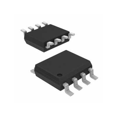
IC OSC SGL TIMER 2.1MHZ 8-SOIC


图片仅供参考.
有关产品详细信息,请参阅产品规格。
IC OSC SGL TIMER 2.1MHZ 8-SOIC
订单满$200即可获赠限量版中式礼品一份.
订单金额超过 1000 美元可减免 30 美元运费.
超过 5000 美元的订单可免运费和交易费.
这些优惠适用于新客户和现有客户,有效期为2024年1月1日至2024年12月31日.
TI
TLC555QDR datasheet
SOP-8
IC芯片
 Lead free/RoHS Compliant
现在提交您的报价请求,我们期望在 五月 03, 2024内提供报价。现在就下订单,我们期望在 五月 08, 2024内完成交易。时间是格林威治标准时间+8:00。


TI
3706 PCS
LDC1314RGHR .PDF
TI
24 PCS
LDC1312DNTR .PDF
TI
90 PCS
LDC1101DRCR .PDF
TI
218 PCS
LD646A .PDF
2024-05-02
Great company- no nonsense
2024-05-02
GREAT COMPANY!!! GREAT QUALITY!! GREAT SERVICE!
2024-05-02
Great Team!!
2024-05-01
Great parts , great price , great service.
2024-04-30
Great supplier over the year!!! we love Gil, Ed, and Karen there.......
2024-04-27
Haim is a great salesperson, one of the best around! Heather Fisher
2024-04-22
It is a pleasure doing business with Censtry.
2024-04-11
I hope we can do more buisness in the Future.
2024-03-21
It was a pleasure to work with Susan at Censtry. Thank you
2024-02-07
John Walsh is great to work and is very professional.
我们高度重视您的反馈意见。请分享您最真实的评价。
*请在发表评论之前登录您的帐户