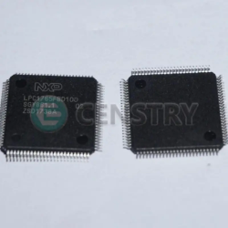
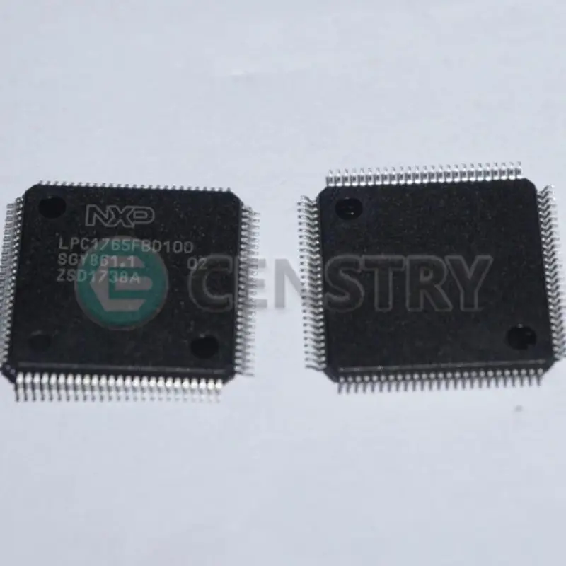
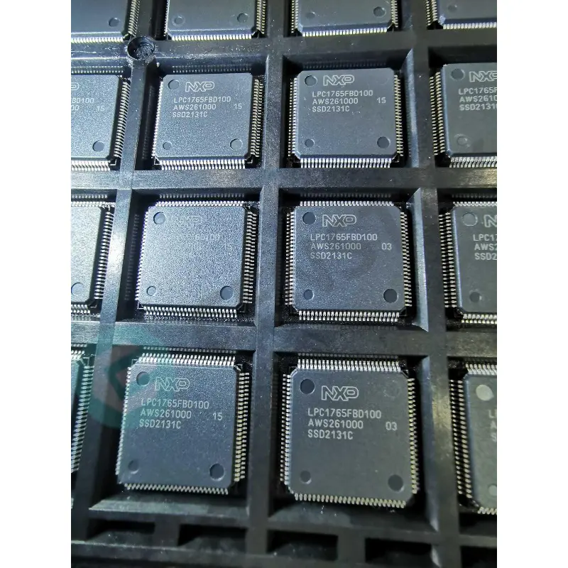
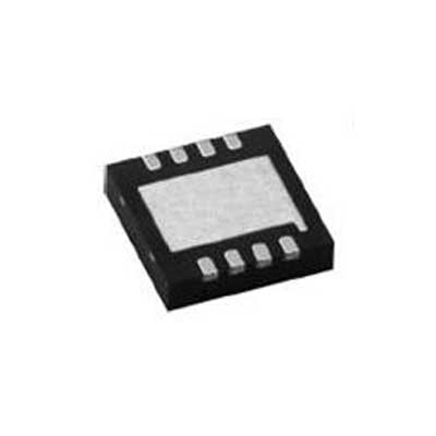
IC MCU 32BIT 256KB FLASH 100LQFP


图片仅供参考.
有关产品详细信息,请参阅产品规格。
IC MCU 32BIT 256KB FLASH 100LQFP
订单满$200即可获赠限量版中式礼品一份.
订单金额超过 1000 美元可减免 30 美元运费.
超过 5000 美元的订单可免运费和交易费.
这些优惠适用于新客户和现有客户,有效期为2024年1月1日至2024年12月31日.
NXP
LPC1765FBD100 datasheet
LQFP-100
IC芯片
 Lead free/RoHS Compliant
现在提交您的报价请求,我们期望在 五月 06, 2024内提供报价。现在就下订单,我们期望在 五月 09, 2024内完成交易。时间是格林威治标准时间+8:00。


1. General description
The LPC1766 is an ARM Cortex-M3 based microcontroller for embedded applications featuring a high level of integration and low power consumption. The ARM Cortex-M3 is a next generation core that offers system enhancements such as enhanced debug features and a higher level of support block integration.
The LPC1766 operates at CPU frequencies of up to 80 MHz. The ARM Cortex-M3 CPU incorporates a 3-stage pipeline and uses a Harvard architecture with separate local instruction and data buses as well as a third bus for peripherals. The ARM Cortex-M3 CPU also includes an internal prefetch unit that supports speculative branching.
The peripheral complement of the LPC1766 includes 256 kB of flash memory, 64 kB of data memory, Ethernet MAC, USB Device/Host/OTG interface, 8-channel general purpose DMA controller, 4 UARTs, 2 CAN channels, 2 SSP controllers, SPI interface, 3 I2C interfaces, 2-input plus 2-output I2S interface, 8 channel 12-bit ADC, 10-bit DAC, motor control PWM, Quadrature Encoder interface, 4 general purpose timers, 6-output general purpose PWM, ultra-low power RTC with separate battery supply, and up to 70 general purpose I/O pins.
The LPC1766 is pin-compatible to the LPC2366 ARM7-based microcontroller.
2. Features
ARM Cortex-M3 processor, running at frequencies of up to 80 MHz. A Memory Protection Unit (MPU) supporting eight regions is included.
ARM Cortex-M3 built-in Nested Vectored Interrupt Controller (NVIC).
256 kB on-chip flash programmimg memory. Enhanced flash memory accelerator enables high-speed 80 MHz operation with zero wait states.
In-System Programming (ISP) and In-Application Programming (IAP) via on-chip boot loader software.
64 kB on-chip SRAM includes: 32 kB of SRAM on the CPU with local code/data bus for high-performance CPU access.
Two 16 kB SRAM blocks with separate access paths for higher throughput. These SRAM blocks may be used for Ethernet, USB, and DMA memory, as well as for general purpose CPU instruction and data storage.
Eight channel General Purpose DMA controller (GPDMA) on the AHB multilayer matrix that can be used with the SSP, I2S, UART, the Analog-to-Digital and Digital-to-Analog converter peripherals, timer match signals, and for memory-to-memory transfers.
Multilayer AHB matrix interconnect provides a separate bus for each AHB master.
AHB masters include the CPU, General Purpose DMA controller, Ethernet MAC, and the USB interface. This interconnect provides communication with no arbitration delays.
Split APB bus allows high throughput with few stalls between the CPU and DMA.
3. Applications
eMetering
Lighting
Industrial networking
Alarm systems
White goods
Motor control
Request a quote LPC1765FBD100 at censtry.com. All items are new and original with 365 days warranty! The excellent quality
and guaranteed services of LPC1765FBD100 in stock for sale, check stock quantity and pricing,
view product specifications, and order contact us:sales@censtry.com.
The price and lead time for LPC1765FBD100 depending on the quantity required, please send your request to us,
our sales team will provide you price and delivery within 24 hours, we sincerely look forward to cooperating with you.
NXP
3265 PCS
NXH5104UK/A1Z .PDF
NXP
2735 PCS
LD6806CX4/18H .PDF
NXP
3757 PCS
LD6806CX4/12H .PDF
NXP
20000 PCS
LD6805K/33H .PDF
2024-05-05
They are very good goods. Thank you!!
2024-05-05
Fast and good as always, thanks!
2024-05-04
Excelent! Everything arrived OK!
2024-05-03
Very fast! Thank you!
2024-05-02
tested, everything ok
2024-04-28
Todo excelentemente bien
2024-04-22
Worked with Matt on first order with firm and found him to be responsive and professional. The company is a pleasure to do business and we will be back again for another deal. Thank you Matt for working with us and insuring our order processed smoothly.
2024-04-08
We have done several deals with Paul over the past 2 years Always a promt reply, friendly service, fast delivery, never a problemwith the quality of the parts.
2024-03-13
Waterlily has sold me a NAIS part 100pcs were perfect,The communication was easy and delivery was on time. We would using them again.
2024-01-19
very professional service . thank you Miss Kelley (eeparts in Shenzhen office ) Thank you for your support . we would like to purchased more electronics components from Miss Kelley . Hope more business each other further
我们高度重视您的反馈意见。请分享您最真实的评价。
*请在发表评论之前登录您的帐户