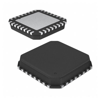
1 Features
• USB2.0 PHY Transceiver Chip, Designed to Interface With a USB Controller via a ULPI Interface, Fully Compliant With:
– Universal Serial Bus Specification Rev. 2.0
– On-The-Go Supplement to the USB 2.0 Specification Rev. 1.3
– UTMI+ Low Pin Interface (ULPI) Specification Rev. 1.1
– ULPI 12-pin SDR Interface
• DP/DM Line External Component Compensation (TI Patent Pending)
• Interfaces to Host, Peripheral and OTG Device Cores; Optimized for Portable Devices or System ASICs with Built-in USB OTG Device Core
• Complete USB OTG Physical Front-End that Supports Host Negotiation Protocol (HNP) and Session Request Protocol (SRP)
• VBUS Overvoltage Protection Circuitry Protects VBUS Pin in Range –2 V to 20 V
• Internal 5 V Short-Circuit Protection of DP, DM, and ID Pins for Cable Shorting to VBUS Pin
• ULPI Interface:
– I/O Interface (1.8V) Optimized for Non-Terminated 50 ΩLine Impedance
– ULPI CLOCK Pin (60 MHz) Supports Both Input and Output Clock Configurations
– Fully Programmable ULPI-Compliant Register Set
• Full Industrial Grade Operating Temperature Range from –40°C to 85°C
• Available in a 32-Pin Quad Flat No Lead [QFN (RHB)] Package
• Can Be Interfaced to Peripheral, Host or OTG Controller Devices via ULPI. Suited to Portable Devices or System ASICs with Built-In Controller Core.
• Complete HS-USB Physical Front-End:
– Supports High Speed (480 Mbit/s), Full Speed (12 Mbit/s) and Low Speed (1.5 Mbit/s)
– Integrated Phase-Locked Loop (PLL) Supporting 2 Clock Frequencies 19.2 MHz/26MHz
– Integrated 45 Ω±10% High-Speed Termination Resistors, 1.5 kΩFull-Speed Device Pull-up Resistor, 15 kΩHost Termination Resistors
– Integrated Transmit and Receive Paths for Parallel-to-Serial and Serial-to-Parallel Data Conversion
– USB Data Recovery to Allow Recovery of USB Data up to ±500 ppm Frequency Drift
– Bit-Stuffing Insertion During Transmit and Removal During Receive
– Non-Return-to-Zero Inverted (NRZI) Encoding and Decoding
– Supports Bus Reset, Suspend, Resume and High-Speed Detection Handshake (Chirp)
– HS USB DP/DM Impedance Programmability for External Component Compensation
• OTG Ver1.3 :
– Control of External VBUS Switch or Charge Pump
– Both Session Request Protocol (SRP) Methods Supported: Data Pulsing and VBUS Pulsing
– Integrated VBUS Detectors and Cable Detection (ID)
• Internal Power-On Reset (POR) Circuit
• Flexible System Integration and Very Low Current Consumption, Optimized for Portable Devices
Request a quote TUSB1210BRHBR at censtry.com. All items are new and original with 365 days warranty! The excellent quality
and guaranteed services of TUSB1210BRHBR in stock for sale, check stock quantity and pricing,
view product specifications, and order contact us:sales@censtry.com.
The price and lead time for TUSB1210BRHBR depending on the quantity required, please send your request to us,
our sales team will provide you price and delivery within 24 hours, we sincerely look forward to cooperating with you.
我们高度重视您的反馈意见。请分享您最真实的评价。
*请在发表评论之前登录您的帐户